FPGA - Design and Engineering
Enable speed, flexibility and hardware-level control
Field Programmable Gate Arrays (FPGAs) provide a unique and flexible route to achieving hardware-level performance and power efficiencies for highly integrated custom designs, without the need for the typically far more time-consuming and costly Application Specific Integrated Circuit (ASIC) design flows.
Why FPGA?
Traditionally, FPGA devices consist of vendor-specific Programmable Logic (PL) fabric which the designer configures according to their specific application requirements using design software. Whilst modern PL-only FPGA implementations are capable of instantiating highly complex functionality, including soft processor cores, many vendors also offer an extensive range of Multi-Processor System on Chip (MPSoC), which augment the traditional PL with a range of hard IP blocks (e.g. Processors, GPU(s), Security, Connectivity) for enhanced functionality and performance.
While ASIC implementations are typically far more cost-effective for very high-volume fixed-functionality custom designs, FPGAs typically provide a much faster development path and, consequently, time-to-market while maintaining a high degree of reconfigurability. This flexibility lies at the very heart of FPGA technology and reinforces its unique value for both final product deployments as well as proving and developing design concepts prior to potential future ASIC implementations.
Our FPGA Expertise
Design Definition
Device Selection
Design Entry & Custom Development
Simulation, Synthesis & Implementation
Device Programming
Tools & Software Development
Capturing and Refining Requirements
A clear understanding of your system needs is the foundation of a successful FPGA design. By thoroughly gathering and analysing these requirements, we ensure that every feature and performance metric is accurately addressed, setting the stage for an efficient and robust solution.
Optimised System and FPGA Architecture
We focus on crafting a performant yet cost-effective architecture by aligning FPGA design considerations with broader system and roadmap objectives. This helps to maximise performance, streamline manufacturing, and support future testing and scalability needs.

Comprehensive Constraints Management
We meticulously capture, validate and review all key functional, performance and cost objectives throughout the development and design verification process. This information forms the basis of a comprehensive test plan to ensure that the final solution remains compliant under all real-world operating conditions.
Rigorous Solution Due Diligence
Throughout the development process, we use a defined test plan to ensure full compliance with all technical requirements. Where appropriate, third-party development board and/or custom PoC designs are often used to complement traditional FPGA design verification techniques, such as timing analysis and test benches, to ensure functionality and reduce risk. This reduces potential setbacks, safeguards against unforeseen complications, and positions your project for success from the outset.
Versatile Development Platforms
Starting with robust proof-of-concept phases, we utilise reliable development platforms to streamline FPGA innovation. This expedites prototyping and testing, ensuring a smooth transition from concept to final product without sacrificing quality or performance.
Strategic Family Selection
Choosing the right FPGA family is crucial for aligning functionality, performance, power, and cost targets. From traditional FPGA families such as Spartan, Artix, Kintex and Vertex to advanced MPSoC solutions such as Zynq and Versal, we evaluate the benefits of each option to match your specific requirements and drive a tailored solution.xi
Targeted MPSoC/FPGA Architectures
When your system demands both processing and programmable logic, MPSoC and FPGA architectures such as Zynq and Artix provide an ideal blend of efficiency and flexibility. Leveraging these architectures optimises processing power and adaptability, catering to the needs of real-time, complex applications.
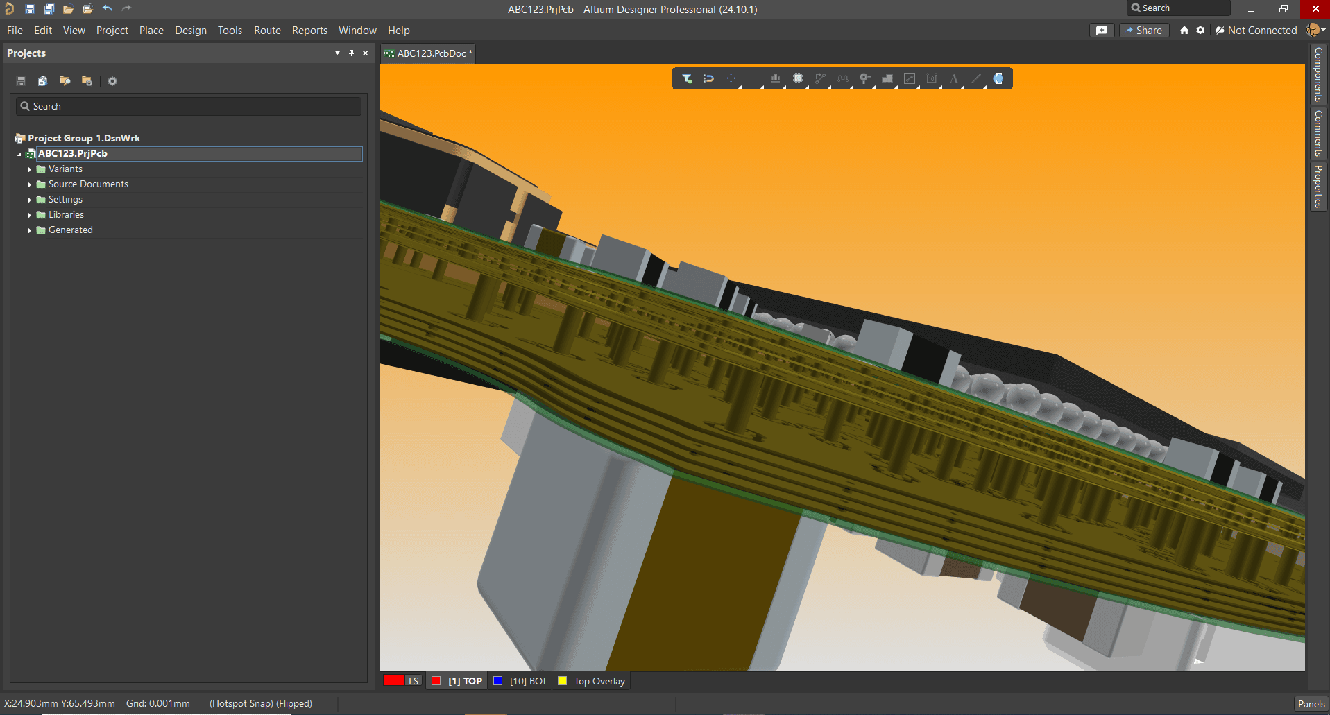
Optimised PCB Layout
We apply best practices in PCB layout design to enhance reliability, performance, and manufacturability while managing space constraints. By focusing on signal integrity, power distribution, and thermal considerations, we ensure your system operates at peak efficiency over its entire lifecycle.
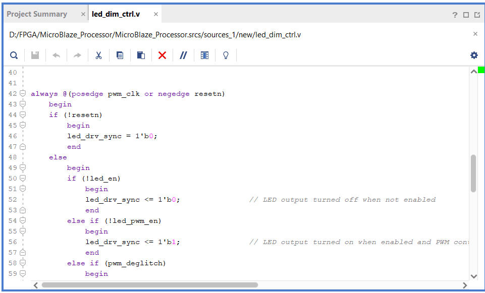
HDL and Schematic-Based Design Entry
We utilise standard-based HDL (Verilog/VHDL) and/or schematic-based approaches to implement structured and hierarchical designs, which are both easy to maintain and transferable.
Robust Clock Tree Definitions
Optimal Clock domain partitioning and clock tree implementation are critical steps to achieving a well-structured design that can meet both the required performance and timing closure. Clock tree management helps mitigate timing issues, reduces jitter, preserves system integrity across diverse operating conditions and supports the most cost-optimal device selection.
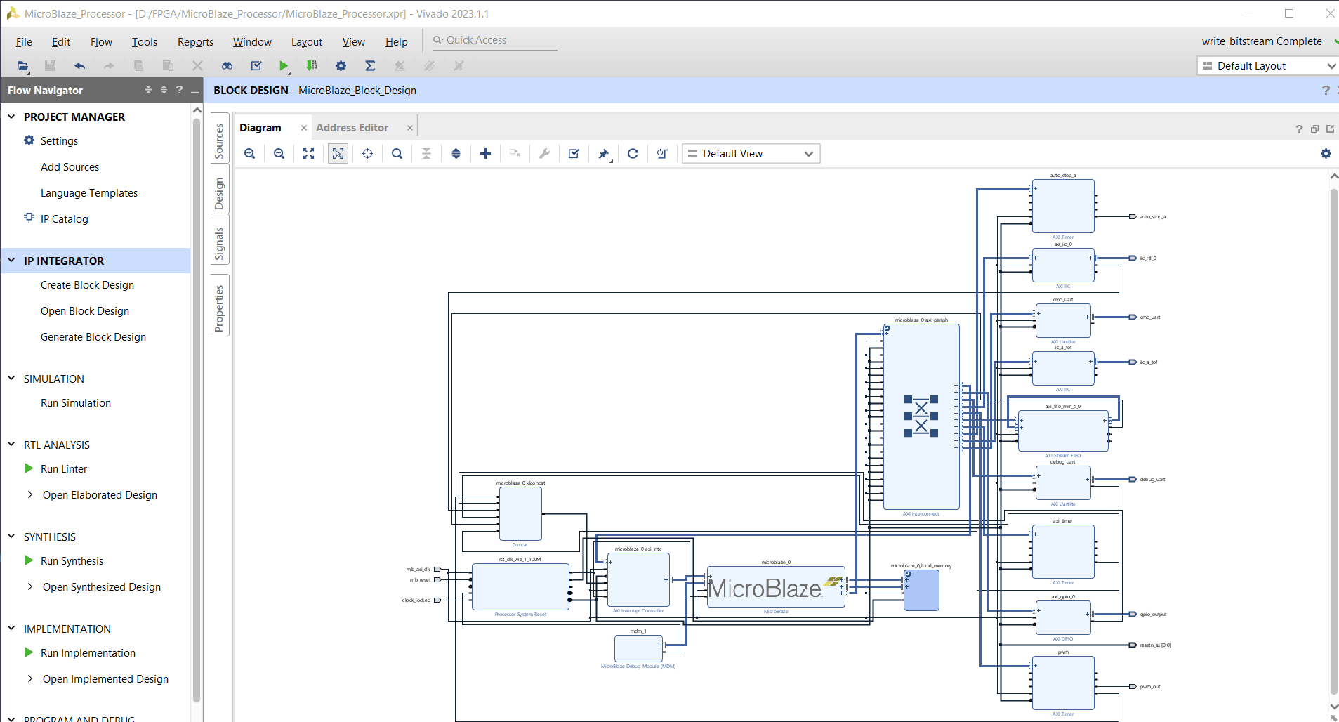
Custom IP Development
When off-the-shelf solutions aren’t enough, we create specialised IP to address unique demands. Our custom development ensures targeted functionality, optimised performance, and greater design flexibility for even the most complex projects.
Third-Party IP Integration
Whether leveraging third-party IP (including AMD (formerly Xilinx) or CAST), we fuse third-party resources into your FPGA design with minimal friction. This accelerates development, helping you reach critical performance milestones more efficiently.
Versatile Soft/Hard Core Processors
We utilise soft/hard core processors (including MicroBlaze™ and ARM) to unlock higher-level functionalities within your FPGA. We deliver adaptable and high-performing solutions by combining advanced computational power with programmable logic.
Test Bench Generation
Test benches play a vital role in verifying design integrity at each stage. Our comprehensive approach to testing catches issues early, ensuring your final product is stable, efficient, and ready for market.
Functional Simulation
By running functional simulations before synthesis, we validate design behaviour and spot any logical inconsistencies. This saves valuable time, ensuring issues are addressed swiftly and without impacting later stages of the development process.
Design Optimisation
We refine your FPGA design during synthesis for optimal power usage and resource allocation. Careful tuning maintains performance goals while minimising energy consumption, leading to a more efficient, cost-effective final product.
Strategic Placement and Floor Planning
Effective placement and floor planning is essential for balancing performance needs with device constraints. Our methodologies reduce routing complexities, helping sustain high clock rates and robust functionality across all operating conditions.
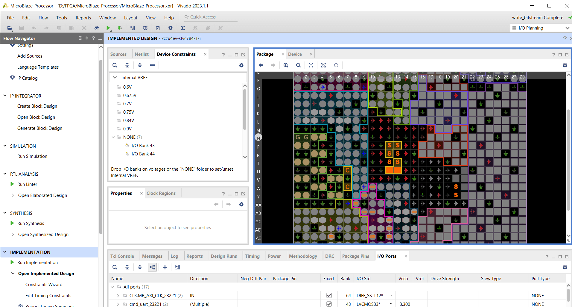
I/O Assignment and PCB Integration
We pay close attention to I/O assignments at both the FPGA and PCB levels, ensuring seamless connectivity and efficient system layout. This synergy between the device and board yields consistent, high-performance results in real-world applications.
Timing Simulation and Closure
Before finalising the design, we perform comprehensive timing simulations and enforce constraints. By validating timing closure, we help guarantee that your solution meets critical performance targets and functions reliably in its intended environment.
Seamless Transition from Development to Deployment
We ensure a seamless transition from prototyping to full-scale production, streamlining device programming throughout each project phase. By maintaining consistency in tools and processes, we help you deploy products faster with minimal risk.
Design Verification
Our thorough design verification confirms that your solution meets all functional and performance goals before final programming. This safeguards against unforeseen challenges that may arise in the future.
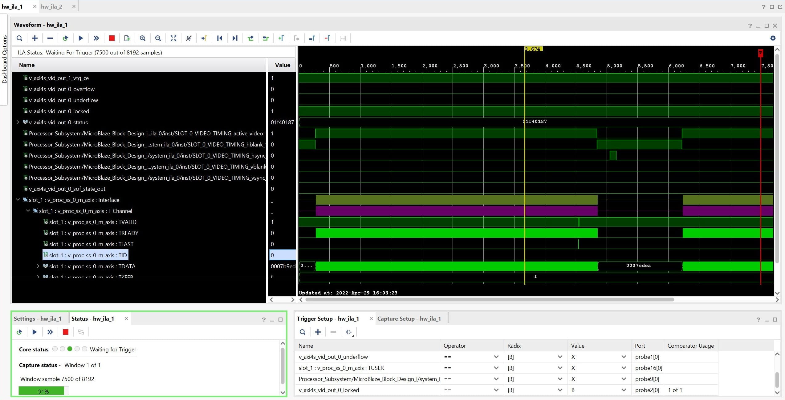
Integrated Logic Analyzer (ILA)
We’ve found on-device ILA instantiation to be an invaluable tool when selectively assessing the real-time functionality, timing analysis and performance of the probed logic, complementing design tool-based functional and timing simulations. Despite consuming FPGA resources, access to on-device ILA information can be an important tool during the design, development and debugging stages, as it helps pinpoint issues quickly.
Debug
We rapidly identify and resolve system anomalies by leveraging advanced debug tools and processes. This maintains quality and stability throughout design iterations.
BSP Generation
Our tailored Board Support Packages expedite your integration process with ready-made hardware support. This reduces development overhead, accelerating time to market through abstraction from the underlying FPGA design.
Security-First Mindset
We protect your IP with robust measures like encryption, secure boot, and end-to-end safeguards. These layered security features mitigate threats and maintain the integrity of your product.
Provisioning
From key assignment to serialisation, we handle all provisioning aspects to ensure device authenticity. This tracking bolsters traceability and strengthens overall system security.
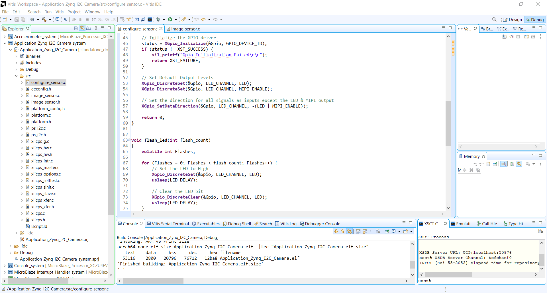
AMD Vivado and Vitis IDE
We utilise AMD (formerly Xilinx) Vivado for streamlined FPGA design and Vitis IDE for integrated software development. This powerful combination ensures a smooth, cohesive workflow, minimising complexities while preserving accuracy and efficiency.
Embedded Software
Whether your project requires bare-metal, RTOS, or Linux environments, our team supports every layer of embedded software development. We tailor solutions to meet your system’s performance, size, and resource demands without compromising reliability.
Boot Loader Development
A well-crafted bootloader is essential for dependable system startup. From the First Stage Boot Loader (FSBL) onward, we carefully manage every aspect of the boot process to ensure secure and efficient processor initialisation and system launch.
Internal and External RAM Execution
We design solutions that effectively utilise both internal and external RAM, offering the best balance of speed, flexibility, and memory capacity. This maintains high system performance while accommodating a range of hardware considerations.
Beyond FPGA: Our full-stack expertise
PCB design & system integration
From package considerations to meticulous pin assignments and advanced via techniques, we provide comprehensive PCB design and seamless system integration.
Our expertise ensures optimal routing, signal integrity, and compatibility with the latest FPGA packages, seamlessly meeting crucial performance and reliability demands.

System architecture
With broad experience across embedded computing, AI, and cloud integration, we design comprehensive, end-to-end architectures for real-world solutions.
Rather than focusing solely on FPGAs, we align every system component for maximum efficiency, allowing seamless interaction and unmatched performance throughout deployment.

Software & AI integration
We offer full stack capabilities supporting FPGA, edge, and cloud environments, from bare metal and RTOS implementations to advanced AI-driven applications.
Our holistic approach enables secure, highly optimised, high-performance solutions, ensuring seamless connectivity and rapid innovation across diverse platforms.
Why partner with Consult Red?
Industry-leading expertise in embedded systems, including FPGA and AI integration.
End-to-end product lifecycle support – from concept to commercialisation.
Proven track record in delivering cutting-edge FPGA-powered solutions.
Ready to discuss your FPGA project requirements?
Please enter your details to request a free consultation, learn more about our FPGA services or partner with us on your next project.

Latest updates

Articles
7 key mistakes businesses make when evolving their Industrial IoT device
In this article, we explore the common mistakes that can derail an Industrial IoT project before it delivers value.

Articles
How to Build Smarter Products Without Starting From Scratch
Innovation is not always about starting again. For many products, there’s a smarter, faster, and more cost-effective path: evolve what already works.

News
Agama and Consult Red announce RDK Accelerator integration
Agama CDM now integrated on RDK Accelerator environment in record time by Consult Red, simplifying future projects.